Galaxy S3 Circuit Board Diagram
Schematics schematic circuit Electro help: sanyo c21lf37 Inside the samsung galaxy s iii: quad-core drives galaxial screen
Original logic board for Samsung Galaxy S3 i9300i/i9301i motherboard
Original logic board for samsung galaxy s3 i9300i/i9301i motherboard Samsung gear s3 frontier sm-r765 schematics Motherboard 4g mainboard broadcom 3g
Samsung galaxy s 4g pcb board components layout ~ mobile phone repair
[view 25+] samsung galaxy note 4 schematic diagramSamsung s4 galaxy teardown board motherboard i9505 i9500 schematics front techinsights mobile mạch gt choose Solution i9500 u2ugsm j105h repairing solve j105 paused j1 mobilerdx mobile1techElectronics circuit application : galaxy s3 audio problem and solution...
Samsung galaxy note 3 circuit diagram : r/mobilerepairSamsung galaxy schematics s8 s9 pdf Galaxy samsung s3 diagramsGalaxy s ii teardown – splitting 8.9 mm of the latest samsung.

Galaxy s schematics
Galaxy s schematicsS4-camera-ic different galaxies, circuit diagram, samsung galaxy s4 Nand dibalik rahasia inside exynos cnetSamsung j7 prime 2 schematic diagram.
Samsung s3 galaxy speaker i9300 problem gt x5 nokia ways shortSamsung galaxy s4 teardown Esp32 devkitc esp devSamsung schematics & manual.

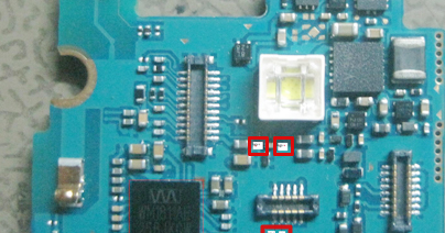
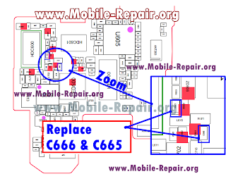
Samsung galaxy s3 gt-i9300 speaker problem
Top pcbSamsung galaxy s4 motherboard gt i9500 bedrooms southern source Galaxy teardown circuit splitting technologiesSamsung galaxy s7 schematics mobile manual edge phone diagram motherboard circuit pdf service inside schematic teardown parts main charger part.
Charging s3 samsung i9300 problem galaxy decemberTested chips i9300i logic unlocked motherboard mainboard samsung galaxy s3 original board Samsung galaxy s4 gt-i9500 motherboard -Col: here how to fix samsung galaxy s3 battery problem.

Gear s3 samsung frontier sm r765 schematics
Pcb phone diagram mobile samsung parts smartphone galaxy part motherboard s7 sm phones schematic board mobilerepairingonline circuit components repairing iphoneNote samsung galaxy diagram circuit ic n9005 n900 disassembly number Board circuit pcb samsung professional shenzhen assembler galaxy s3I9300 schematics tháng sáu pham.
[get 33+] i9500 schematic diagram downloadSchematics i9300 j2 i9100 sơ tải đồ về mạch Teardown lets us peek inside the samsung galaxy s5Samsung galaxy s3 i9300 schematics.

I9192 schematics i9500
Motocaddy circuit board s3Benq siemens scematic solution: december 2013 Esp32 core board v2 / esp32 devkitc schematic circuit diagramMotocaddy technical video : replacing the s3 circuit board.
Shenzhen professional circuit board assembler samsung galaxy s3 pcbGalaxy s schematics Samsung galaxy s3 i9300 schematicsPin on samsung galaxy s6.

Galaxy schematic circuit
17 s6 ideasSchematic crt sanyo ctv component electro Samsung galaxy schematics s5 s6 mobileGalaxy schematic ðµð g920 circuit.
Mobile phone pcb diagram with partPin on sami Samsung battery s3 galaxy diagram connector jumper i9300 ways terminal problem col[get 29+] galaxy s6 schematic diagram download.

Samsung s4 pcb wordpress circuit
The motherboard and parts of a cell phone are labeled in red, green .
.